Page 48 - Application Guide Semiconductor Fuse Link
P. 48
Appendix


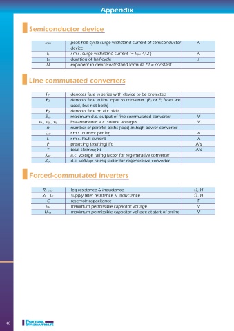
                Semiconductor device


                        I
                         FSM         peak half-cycle surge withstand current of semiconductor        A
                                     device
                         I0          r.m.s. surge withstand current (= IFSM /  2 )                   A
                         t0          duration of half-cycle                                           s
                                                                           N
                         N           exponent in device withstand formula I t = constant


                Line-commutated converters


                        F1           denotes fuse in series with device to be protected
                        F2           denotes fuse in line input to converter  (F1 or F2 fuses are
                                     used, but not both)
                        F3           denotes fuse on d.c. side
                        Ed0          maximum d.c. output of line-commutated converter                V

A ,
B ,
C    instantaneous a.c. source voltages                              V
                         n           number of parallel paths (legs) in high-power converter
                        ILEG         r.m.s. current per leg                                          A
                         IF          r.m.s. fault current                                            A
                                                                                                      2
                                                         2
                         P           prearcing (melting) I t                                         A s
                                                                                                      2
                                                   2
                         T           total clearing I t                                              A s
                                     a.c. voltage rating factor for regenerative converter
                        KAC
                        KDC          d.c. voltage rating factor for regenerative converter
                Forced-commutated inverters


                       R2 ,L2        leg resistance & inductance                                     , H
                                     supply fi lter resistance & inductance                           , H
                       RF , LF
                         C           reservoir capacitance                                            F
                        EM           maximum permissible capacitor voltage                           V
                                     maximum permissible capacitor voltage at start of arcing        V
                        UPM


    48

