Page 34 - Semi Conductor use application guide
P. 34
Forced commutated inverters


                Fuse insertion inductance


                 Semiconductor fuses are increasingly being used to protect IGBT inverters against the effects of short-
                 circuit faults. These circuits switch at high frequencies, typically around 10kHz. At these frequencies
                 the switching  di/dt is high, and the circuit inductance must be kept low to minimize transient
                 over-voltages. The effect of the insertion of a fuse on the circuit inductance can be an important
                 consideration in circuit design. The additional induction caused by the insertion of a fuse is mainly
                 due to the modifi cation to the circuit loop. The internal self-inductance of the fuse is negligible.


                Minimizing the circuit inductance


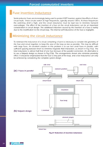
                 To minimize the inductance of a circuit containing a fuse it is necessary to consider the geometry of
                 the fuse and circuit together, to keep the area of the loop as low as possible. This may be diffi cult
                 with large fuses. An excellent solution to this problem is to use two small fuses in parallel, with
                 suffi cient spacing between them to minimize magnetic fi eld interaction, as shown in Fig.27(a). The
                 total inductance is almost half that of one fuse because of the parallel connection. An alternative is
                 to use a fl atpack design as shown in Fig.27(b). The arrangements shown also minimize proximity
                 effect. It should be emphasized that the fuse is only part of the loop, and a low inductance can only
                 be achieved by considering the complete system design.


                                                   side view                                 end view

                                                                 element position
                 (a) 2 fuses in parallel


                                                  circuit boad                           return bus


                                                                        insulation


                                                                       fuse body


                                                 L terminal
                 (b) fl atpack design


                                                                         element strip(s)


                                              return bus

                                                          Fig.27 Reduction of insertion inductance


    34

