Page 23 - Application Guide Semiconductor Fuse Link
P. 23
3-phase controlled bridge rectifi er


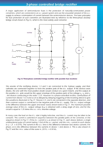
        A major application of semiconductor fuses is the protection of naturally-commutated power
        converters, which are connected to an a.c. power system and use the sinusoidal variation of the a.c.
        supply to achieve commutation of current between the semiconductor devices. The basic principles
        for fuse protection of such converters are illustrated here by reference to the three-phase (Graetz)
        bridge circuit shown in Fig.16, which is the most widely used converter.


                                                                                  F3

                                                                              5
                                0.577id          1              3

                                                                                                 Id
                                                 F1
                                 F2
               a


               b                                                                           DC


               c


               AC             0.816Id
               Supply
                                                 2             4              6


                     Fig.16 Three-phase controlled bridge rectifier with possible fuse locations


        The anodes of the rectifying devices 1,3 and 5 are connected to the 3-phase supply, and their
        cathodes are connected together to form the positive pole of the d.c. output. If the devices were
        diodes, the one with the most positive anode would conduct at a given instant, and the output at
        the positive d.c. pole would be the upper envelope of the positive parts of the voltage
 ,
  and
                                                                                               A  B      C
        , the devices conducting in the order 1,3,5. However in a phase-controlled rectifi er, commutation of
        current from device 1 to 3 and so on is delayed by delaying triggering of the incoming device to give
        the waveforms illustrated in Fig.17. Devices 2,4, and 6 are connected in the opposite direction, and
        their common output is connected to the negative pole of the d.c. supply. The d.c. output voltage
        is the difference between the upper and lower waves shown bold in Fig.17. The maximum possible
        average value of the d.c. output voltage (Ed0) is obtained with a delay angle of zero, and for this
        circuit is equal to 1.35 times the a.c. r.m.s. line-line voltage.


        In many cases the load on the d.c. side is highly inductive, and the d.c. current may be taken to be
        constant. This current is switched in sequence between the parallel paths of the converter, in the
        sequence shown in Fig.17. If the d.c. current is Id as shown in Fig.17, each device delivers a single
        unidirectional pulse of current lasting 1/3rd of the a.c. period, and the r.m.s. current in each device
        is Id /  3  = 0.577Id. The current in the a.c. lines is the difference between two device currents. For
        phase a it is the difference between the currents in device 1 and device 2. This is also shown in
        Fig.17 and the r.m.s. value of this wave is  2/3 Id  = 0.816Id.


                                                                                                                   23

