Page 32 - Application Guide Semiconductor Fuse Link
P. 32
Forced commutated inverters


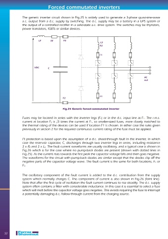
                 The generic inverter circuit shown in Fig.25 is widely used to generate a 3-phase quasi-sine-wave
                 a.c. output from a d.c. supply by switching. The d.c. supply may be a battery in a UPS system or
                 the output of a controlled rectifi er in a solid-state a.c. drive system. The switches may be thyristors,
                 power transistors, IGBTs or similar devices.


                            LF       RF       F2
                                                                        L2
                                                                        R2


                                                                        F1


                         VDC       C


                                                                                                       AC
                                                                                                       out


                                                                        F1
                                              F2


                                             Fig.25 Generic forced-commutated inverter

                 Fuses may be located in series with the inverter legs (F1) or in the d.c. input line at F2. The r.m.s.
                 current at location F2 is  3 times the current at F1, so smaller-sized fuses, more closely matched to
                 the thermal rating of the devices can be used if location F1 is chosen. In either case the rules given
                 previously in section 2 for the required continuous current rating of the fuse must be applied.


                 2
                 I t protection is based upon the assumption of a d.c. shoot-through fault in the inverter, in which
                 case the reservoir capacitor, C, discharges through two inverter legs in series, including resistance
                 2 x R2 and 2 x L2. The fault current waveforms are usually oscillatory, and a typical case is shown in
                 Fig.26 which is for the case where no pump-back diodes are present (shown with dotted lines in
                 Fig.25). As the current rises towards the fi rst peak the capacitor voltage falls and then goes negative.
                 The waveforms for the circuit with pump-back diodes are similar except that the diodes clip off the
                 negative parts of the capacitor voltage wave. The fault current is the same for both locations, F1 or
                 F2.


                 The oscillatory component of the fault current is added to the d.c. contribution from the supply
                 system which normally charges C. This component of current is also shown in Fig.26 (faint line).
                 Note that after the fi rst cycle of oscillation the fault current continues to rise steadily. The d.c. supply
                 system often contains a fi lter with considerable inductance. In this case it is essential to select a fuse
                 which will melt before the capacitor voltage goes negative. This avoids requiring the fuse to interrupt
                 a potentially damaging d.c. follow-through current from the charging source.


    32

